
The Chip Design and Fabrication using VLSI Domain offers exciting growth opportunities for engineers who are strong in electronic design fundamentals, have an interest in VLSI design and verification and know how to apply VLSI concepts to practice.VLSI professionals are always in high demand in the fast-changing chip designing industry.
Domain Track: Chip Design and Fabrication using VLSI
Domain Track: Chip Design and Fabrication using VLSI
Course Attendees
Still no participant
Course Reviews
Still no reviews
Track Total Credits: 18 (6-6-6)
Domain Code : VLCU2070
Courses Division:
- ASIC Design (2-1-0)
- Digital VLSI (2-2-0)
- Analog VLSI (2-1-0)
- Verification Using SystemVerilog (0-2-0)
- Project (0-0-6)
Domain Track Objectives
The Chip Design and Fabrication using VLSI is a skill-based industry integrated domain course. It is delivered in a unique experiential learning process of interactive hands-on sessions, beginning with essential theoretical foundations, and progressing to learning how to effectively apply them in the real world.To facilitate effectivelearning, this is accompanied by laboratory sessions using EDA tools and FPGA development boards, mentor support, and case studies.
- This course would enable students to design analog / digital IC components, design of application-specific integrated circuits (ASICS) for digital systems and theory and practice of VLSI test and verification.
- To study the issues relating to the design of application-specific integrated circuits (ASICS) for digital systems.
- To involve the students in the theory and practice of VLSI test and verifications.
Domain Track Learning Outcomes
- On accomplishment of this course the students will be familiar with modern VLSI circuits and will be able to design most of them.
- Students will demonstrate an understanding of issues involved in ASIC design, including technology choice, Timing analysis, tool-flow, testability.
- Students will become an Industry-ready RTL Design/Physical design/Testing/Verification Engineer.
Career Scope
- Register transfer level (RTL) design and verification Engineer
- Physical design and verification Engineer
- Analogue and mixed signal CMOS IC design Engineer
- CAD tool Developer
- Higher studies and Research
- Self-employment through entrepreneurship
Domain Syllabus
1. ASIC Design (2-1-0)
- 1.1 Custom IC Design, Cell-Based Design Methodology, Array Based Implementation Approaches.
- 1.2 Traditional and Physical Compiler Based ASIC Flow
- 1.3 Logic Synthesis Environment
- 1.4 Technology library: technology libraries, logic library basics, delay calculations
- 1.5 Static Time Analysis , Critical Path, Timing Exceptions
- 1.6 Multi Cycle Paths, False Paths and Timing Constraints
- 1.7 Floor Planning Place and Route Optimization
- 1.8 Partitioning: Partitioning For Synthesis and coding guidelines
- 1.9 Optimization and Mapping Constraints (Clock, Delay, Area, Design)
- 1.10 Design Methodology for Logic Cores
- 1.11 Architecture of The Present-Day Soc
- 1.12 Design Issues of SoC, Hardware &
- 1.13 Software Design, Core Libraries
- 1.14 EDA Tools SoC Design Flow Guidelines for Design Reuse
- 1.15 Design Process for Soft and Firm Cores
- 1.16 Design Process for Hard Cores, System Integration
- 1.17 Design Methodology for Memory & Analog Cores Embedded Memories
- 1.18 Design Methodology for Embedded Memories
- 1.19 Specification of Analog Circuits
- 1.20 Core Level Validation, Core Interface
- 1.21 Verification, SoC Design Validation
Text Books:
- Verilog HDL, 2/E By Samir Palnitkar, Pearson Education
- Himanshu. Bhatnagar, “Advanced ASIC Chip Synthesis” (2/e).KAP.2002
- Rochit Rajsuman, ‘System-on-a-Chip: Design and Test’, Artech House, 2000
Reference Books:
- Maheshwari, Naresh, Sapatnekar, “Timing Analysis and Optimization of Sequential Circuits”. 1998, Springer. ISBN: 978-0-7923-8321-5
- Modern Digital Electronics. Author, R P Jain. Edition, 3. Publisher, Tata McGraw-Hill Education
Software Tool:
- Microwind
- Cadence
- Xilinx ISE
2.Digital VLSI (2-2-0)
- 2.1 Issues in Digital IC Design
- 2.2 Quality Metrics of A Digital Design
- 2.3 Manufacturing CMOS Integrated Circuits
- 2.4 Design Rules. Layouts
- 2.5 The Metal Oxide Semiconductor (MOS) Structure
- 2.6 The MOS System Under External Bias
- 2.7 Structure And Operation of MOS Transistor (MOSFET)
- 2.8 MOSFET Current-Voltage Characteristics
- 2.9 MOSFET Scaling And Small-Geometry Effects, MOSFET Capacitance
- 2.10 Static CMOS Inverter: Static And Dynamic Behavior Practices of CMOS Inverter
- 2.11 Components Of Energy And Power: Switching, Short-Circuit And Leakage Components
- 2.12 Technology Scaling And Its Impact On The Inverter Metrics
- 2.13 Static CMOS Design: Complementary CMOS, Ratioed Logic, Pass Transistor Logic
- 2.14 Dynamic CMOS Design: Dynamic Logic Design Considerations
- 2.15 Speed And Power Dissipation Of Dynamic Logic
- 2.16 Signal Integrity Issues, Cascading Dynamic Gates
- 2.17 CMOS Sequential Logic Circuit Design Introduction, Bi-Stable Circuit Elements
- 2.18 SR & JK Latch Circuits
- 2.19 Clocked Latch And Flip-Flop Circuits
- 2.20 CMOS D-Latch And Edge-Triggered Flip-Flop
- 2.21 Semiconductor Memory Design: Introduction, MOS Decoders
- 2.22 SRAM Design, DRAM Design
- 2.23 Memory Architecture And I/O Circuitry
Text Books:
- Sung-Mo Kang and Yusuf Leblebici, CMOS Digital Integrated Circuits: Analysis and Design, Tata McGraw-Hill Publishing Company Limited
- Jan M,Rabaey, AnanthaChandrakasan, BorivojeNikolic, Digital Integrated Circuits–A Design Perspective, PHI
Reference Books:
- Wayne Wolf, Modern VLSI Design System – on – Chip Design, PHI
- K,Eshraghian and N,H,E,Weste, Principles of CMOS VLSI Design – a Systems Perspective, 2nd Edn,, Addison Wesley
Software Tool:
- Microwind
- Cadence
3.Analog VLSI (2-1-0)
- 3.1 Independent Sources: MOS Current Sources and Sinks
- 3.2 Current Mirror: Basic Current Mirrors, Cascode Current Mirrors
- 3.3 Current and Voltage Reference Circuits
- 3.4 Amplifier Design : Basic Concepts of Amplifier, Common Source Stage
- 3.5 Common Gate Stage, Cascode Stage
- 3.6 Differential Stage: Single Ended and Differential Operation
- 3.7 Basic Differential Pair
- 3.8 Frequency Response of Amplifiers: Miller Effect, Frequency Response of Common Source Stage
- 3.9 Common Gate Stage, Cascode Stage and Differential Pair
- 3.10 CMOS Op-Amps: Differential and Common Mode Circuits
- 3.11 Op-Amp CMRR Requirements, Need for Single and Multistage Amplifiers
- 3.12 Effect of Loading in Differential Stage
- 3.13 Digital To Analog Converters:( Binary Weighted Resistor, R-2R Ladder Network)
- 3.14 Analog To Digital Converters: (Dual Slope, Successive Approximation Type)
- 3.15 Frequency Compensation: Concepts and Techniques for Frequency Compensation
- 3.16 Dominant Pole, Miller Compensation, Compensation of Miller RHP Zero
- 3.17 Nested Miller, Compensation of Two Stage OP-Amps
Text Books:
- Behzad Razavi, “Design of Analog CMOS Integrated Circuits”, McGraw-Hill, 2000.
- Phillip E. Allen and Douglas R. Holberg, “CMOS Analog Circuit Design”, (Second Edition) Oxford University Press, February 2002.
Reference Books:
- Gray, Hurst, Lewis, and Meyer: “Analysis and design of Analog Integrated Circuits”, (4/e), John Wiley and Sons.
Software Tool:
- Microwind
- Cadence
4.Verification Using SystemVerilog (0-2-0)
- 4.1 Verification Concepts
- 4.2 Introduction to System Verilog Language
- 4.3 Basic SV TB - Connecting to your design
- 4.4 SV-OOPs concepts and Randomization
- 4.5 Threads and Inter Process Communication
- 4.6 Introduction to Verification Methodologies
- 4.7 Case Study : Design and Verification of a SRAM Memory Cell Using UVM Methods
Software Tool:
- Questa Sim
Text Books:
- Sutherland, Stuart, Simon Davidmann, and Peter Flake, “SystemVerilog for Design Second Edition: A Guide to Using System Verilog for Hardware Design and Modeling”, Springer Science & Business Media, 2006
- Spear, Chris. “SystemVerilog for verification: a guide to learning the testbench language features,” Springer Science & Business Media, 2008
Reference Books:
- System Verilog, 3.1a, Language reference manual
- Vijayaraghavan, Srikanth, and Meyyappan Ramanathan. A practical guide for SystemVerilog assertions. Springer Science & Business Media, 2005
- Bergeron, J. "Writing Testbenches Using SystemVerilog.―NY: Springer Science and Business Media." (2006)
Web Source:
Session Plan:
ASIC Design: (2-1-0)
Session 1: Introduction
- Lecture Note: Introduction....

Session 2: ASIC Design Flow.
- Lecture Notes: Digital VLSI Design Flow...
- Video Link: ...

Session 3: Practice:
- EDA Tools : Cadence
- Design Project Organization
Tools Used: Cadence EDA
Session 4: Introduction to FSM, Mealy and Moore Models.
Session 5: Architecture Area, Architecture speed, Architecture Power
Session 6: Practice
- Starting The Design Vision Graphical Environment
- RTL Model Analysis
- Design Elaboration
Tool Used:
- Cadence EDA
Session 7: Introduction to RTL
- Lecture Note: Introduction to RTL...
- Video Link: ...
Session 8: Static Timing Analysis
- Lecture Note: Static Timing Analysis...
- Video Link: ...
Session 9: Practice:
- RTL Design of Pipelined Architecture and Its Performance Evaluation
- Design Constraint Definitions
- Design Mapping and Optimization
Tool Used: Cadence EDA
Session 10: RTL Coding for Synthesis
- Lecture Note: RTL Coding for Synthesis...
- Video Link: ...
Session 11: Floorplanning
- Lecture Note: Floorplanning (Part-1)...
- Video Link: ...
Session 12: Practice
- RTL Design of ALU Architectures
- Static Timing Analysis of ALU
Tool Used: Cadence EDA
Session 13: Floorplanning (Contd..)
- Lecture Note: Floorplanning (Part-2)...
- Video Link: ...
Session 14: Placement
- Lecture Note: Placement...
- Video Link: ...
Session 15: Practice
- Starting The Encounter Graphical Environment
- Design Import
- Global Net Connections
Tool Used:
- Cadence EDA
Session 16: Routing optimization
- Lecture Note: Routing optimization...
- Video Link: ...
Session 17: Introduction to SOC
- Lecture Note:Introduction to SoC...
- Video Link: ...
Session 18: Practice
- Floorplan Specification
- Power Ring/Stripe Creation And Routing
- Core Cell Placement
Tool Used:
- Cadence EDA
Session 19: SoC Models
- Lecture Note: SoC Models...
- Video Link: ...
Session 20: SoC Design Process
- Lecture Note: SoC Design Process...
- Video Link: ...
Session 21: Practice
- Design Checks
- Report Generation
- Tool Used: Cadence EDA
Session 22: SoC Characteristics
- Lecture Note: SoC Characteristics...
- Video Link: ...
Session 23: System Level Design Issues
- Lecture Note: System Level Design Issues...
- Video Link: ...
Session 24: Practice
- Post-Route Timing Data Extraction
- Post-Route Netlist Generation
- GDSII File Generation
Tool Used:
- Cadence EDA
Session 25: System Verification
- Lecture Note: System Verification...
- Video Link: ...
Session 26: System Inter Connection
- Lecture Note: System Inter Connection...
- Video Link: ...
Session 27: Design for Test
- Lecture Note: Design for Test...
- Video Link: ...
Session 28: Practice
- Design of FIFO Register using Cadence (Both Frontend and Backend)
- Tool Used: Cadence EDA
Session 29: MACRO Design and Integration
- Lecture Note: MACRO Design Integration...
- Video Link: ...
Session 30: Design of Logic Cores
- Lecture Note: Design of Logic Cores...
- Video Link: ...
Digital VLSI (2-2-0)
Session 1: Introduction
- Lecture Note: Introduction ...
- Video Link: ...
Session 2: CMOS Fabrication
- Lecture Note CMOS Fabrication ...
- Video Link: ...
Session 3:Practice
- Layout design of NMOS and PMOS transistor
- Layout design of CMOS inverter
Tool Used:
- CADENCE EDA
Session 4: CMOS Layout
- Lecture Note: CMOS Layout ...
- Video Link: ...
Session 5: CMOS Layout (Contd..)
- Lecture Note: CMOS Layout (Contd..) ...
- Video Link: ...
Session 6:Practice
- Study of Full-custom IC Design flow: Schematic simulation, DRC, LVS, QRC, Post Layout Simulation.
- Study of NMOS and PMOS drain current characteristics and transfer characteristics.
Tool Used:
- Cadence EDA
Session 7:MOS Structure and Region of Operation
- Lecture Note: MOS Structure ...
- Lecture Note: NMOS Resistive region Operation ...
- Video Link: ...
Session 8: MOS Short Channel effects
- Lecture Note: MOS Short Channel Effect ...
- Lecture Note: Channel Length Modulation ...
- Video Link 1: ...
- Video Link 2: ...
Session 9: Practice
- Extraction of device model parameters.
- Introduction to layout editor and Layout of NMOS and PMOS transistor.
Tool Used:
- Cadence EDA
Session 10: MOS Capacitance
- Lecture Note: MOS Capacitance ...
- Video Link: ...
Session 11: CMOS Inverter and VTC
- Lecture Note: CMOS Inverter ...
- Lecture Note: CMOS VTC ...
- Video Link 1: ...
- Video Link 2: ...
Session 12: Practice
- Study of resistive load and enhancement load Inverter static characteristics.
- Study of CMOS inverter transfer characteristics.
Tool Used:
- Cadence EDA
Session 13: CMOS Inverter Delay and Sizing
- Lecture Note: CMOS Inverter Delay ...
- Lecture Note: Inverter Sizing ...
- Video Link: ...
Session 14: Power Dissipation
- Lecture Note:1 Power Dissipation ...
- Lecture Note:2 Power Dissipation ...
- Video Link: ...
Session 15: Practice
- Study of variation of VTC curve with different MOS transistor size.
Tool Used:
- Cadence EDA
Session 16: Static and Complementary CMOS Logic
- Lecture Note: Static CMOS Circuit ...
- Lecture Note: Complementary CMOS Logic ...
- Video Link 1: ...
- Video Link 2: ...
Session 17: Stick Diagram and Euler Path
- Lecture Note: Stick Diagram ...
- Lecture Note: Euler Path ...
- Video Link: ...
Session 18: Practice
- Design and simulation of NAND and NOR gate and study of static characteristics.
- Design and Simulation of complex CMOS logic circuits: half adder, full adder, 2:1 MUX and 4:1 MUX
Tool Used:
- Cadence EDA
Session 19: Ratioed and Pass Transistor Logic
- Lecture Note: Ratioed Logic ...
- Lecture Note: Pass Transistor Logic ...
- Video Link: ...
Session 20: Dynamic Logic and Logical Effort
- Lecture Note: Dynamic Logic ...
- Lecture Note: Logical Effort ...
- Video Link: ...
Session 21: Practice
- Study of NMOS and PMOS pass transistor characteristics.
- Study of transmission gate characteristics.
Tool Used:
- Cadence EDA
Session 22: Dominos Logic
- Lecture Note: Dominos ...
- Video Link: ...
Session 23: Sequential Logic and Bistable Elemnent
- Lecture Note: Sequential Logic Circuit ...
- Lecture Note: Bistable Elements ...
- Video Link: ...
Session 24: Practice
- Design and simulation of latch circuit.
- Master-slave edge triggered D flip-flop using multiplexer.
Tool Used:
- Cadence EDA
Session 25: CMOS Latch and Flip-Flop
- Lecture Note: SR & JK Latch Circuit ...
- Lecture Note: Edge Trigger Flip-Flop ...
- Video Link: ...
Session 26: Memory Architecture
- Lecture Note: Memory Architecture ...
- Video Link: ...
Session 27: Practice
- Study of CMOS inverter transient characteristics with no load. Calculation of rise time and fall time.
- Study of CMOS inverter delay with different capacitive load.
- Inverter design with delay constraint and simulation.
Tool Used:
- Cadence EDA
Session 28: Memory: SRAM Design
- Lecture Note: SRAM Design ...
- Video Link: ...
Session 29: DRAM Design and Sense Amplifier
- Lecture Note: DRAM Design ...
- Lecture Note: Sense Amplifier ...
- Video Link: ...
- Video Link: ...
Session 30: Practice
- Design and analysis of 6-T conventional SRAM cell.
- Design and analysis of DRAM cell.
Tool Used:
- Cadence EDA
Analog VLSI(2-1-0)
Session 1: Introduction to MOS
- Lecture Note: Introduction to MOS ...
- Video Link: ...
Session 2: Independent Sources
- Lecture Note: Independent Sources ...
- Video Link: ...
Session 3: MOS Transcoductance
- Lecture Note MOS Transconductance ...
- Video Link: ...
Session 4: Practice:
- Study of VLSI CAD Tools (Working Environment, Introduction to Vi Editor, Cadence Virtuoso Simulator.
Tool Used:
- Cadence EDA
Session 5: 3.4 Amplifier Applications
- Lecture Note: Amplifier Applications ...
- Video Link: ...
Session 6: Common Source Amplifier
- Lecture Note: Common Source Amplifier ...
- Video Link: ...
Session 7: Common Source Amplifier (Contd..)
- Lecture Note: Common Source Amplifier ...
- Video Link: ...
Session 8: Practice
- Design of Common Source Amplifier.
Tool Used:
- Cadence EDA
Session 9: Source Follower
- Lecture Note: Source Follower ...
- Video Link: ...
Session 10: Common Gate
- Lecture Note: Common Gate ...
- Video Link: https://www.youtube.com/watch?v=Fh-Xhc88P2E
Session 11: Cascode Stage
- Lecture Note: Cascode Stage ...
- Video Link: ...
Session 12: Practice
- Design of Two Stage Amplifier and Frequency Response Analysis.
Tool Used:
- Cadence EDA
Session 13: Differential Amplifier
- Lecture Note: Differential Amplifier ...
- Video Link: ...
Session 14: Differential Pair with MOS Loads
- Lecture Note: Differential Pair with MOS Load ...
- Video Link: ...
Session 15: Small Signal Analysis of Common Source
- Lecture Note: Common Source ...
- Video Link: ...
Session 16: Practice
- Design of Multi Stage Operational Amplifiers and Study of Loading Effect.
Tool Used:
- Cadence EDA
Session 17: Small Signal Analysis of Common Gate
- Lecture Note: Small Signal Analysis(Common Gate) ...
- Video Link: ...
Session 18: Small Signal Analysis of Common Drain
- Lecture Note: Small Signal Analysis (Common Drain) ...
- Video Link: ...
Session 19: Design of Two Stage CMOS Op-Amp
- Lecture Note: Design of Two Stage CMOS op-amp ...
- Video Link: ...
Session 20: Practice
- Determination Poles and Zeros of Amplifier Circuits.
Tool Used:
- Cadence EDA
Session 21: Design of Two Stage CMOS Op-Amp (Contd..)
- Lecture Note: Design of Two Stage CMOS op-amp ...
- Video Link: ...
Session 22: Frequency Compensation of CMOS Op-Amp
- Lecture Note: Frequency Compensation ...
- Video Link: ...
Session 23: Frequency Compensation of CMOS Op-Amp (Contd..)
- Lecture Note: Frequency Compensation ...
- Video Link: ...
Session 24: Data Converter (ADC)
- Lecture Note: ADC ...
- Video Link: (Successive Approximation) ...
- Video Link: (Counter Type) ...A2pG6Vc
Session 25: Data Converter (DAC)
- Lecture Note: DAC ...
- Video Link: ...
Verification Using SystemVerilog (0-2-0)
Practice Sessions:
Session 1: Verification Concepts (2 Hrs.)
Session 2: Introduction to System Verilog Language (2 Hrs.)
Session 3: Basic SystemVerilog Testbench - Connecting to your design (2 Hrs.)
Session 4: SystemVerilog-OOPs concepts and Randomization (2 Hrs.)
Session 5: Threads and Inter Process Communication (2 Hrs.)
Session 6: Introduction to Verification Methodologies:UVM (2 Hrs.)
Case Study (12 Hrs.)
- Constructing UVM Testbench for SRAM Memory Cell
Project (0-0-6)
List of Projects to be done in domain:
- 1.Design and Development of Shakti Processor
- 2.Design and Implementation of Memristor Based DAC
- 3.ASIC Implementation of RISC5 Processor
- 4.Design and Implementation of Data Acquisition System
- 5.FPGA Implementation I2C Protocol
Gate Process for Project
Gate 0:
- Project Objective
Gate 1:
- Scope
- Project Scope Video ...
Gate 2:
- Development (Work Breakdown Structure)
- Project Life Cycle (Video)...
- Work Breakdown Structure(Video)...
Gate 3:
- Testing and Validation
Gate 4:
- Documentation
Design flows


Software and Hardware
1. EDA Tools

Cadence EDA Tool

Vivado Design Suite
Xilinx ISE

BlueSpec Compiler

Verilator
2. FPGA Development Boards

ARTY A7-100T FPGA Development Board

EDGE ZYNQ FPGA Development Board
Student Projects
Latest News & Student Testimonials
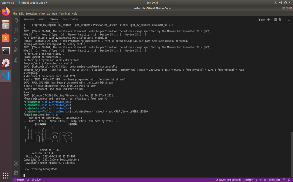
Ongoing Project on Physical Design of Chromite MSOC in collaboration with Incore Semiconductor Pvt. Ltd.
This project envisages the Physical Design of Chromite MSOC which is based on 64-bit RISC-V architecture. The design process includes steps such as hardening and adding DFT support for chromite pipeline. Tools Used: Cadence EDA Tool, BSV compiler
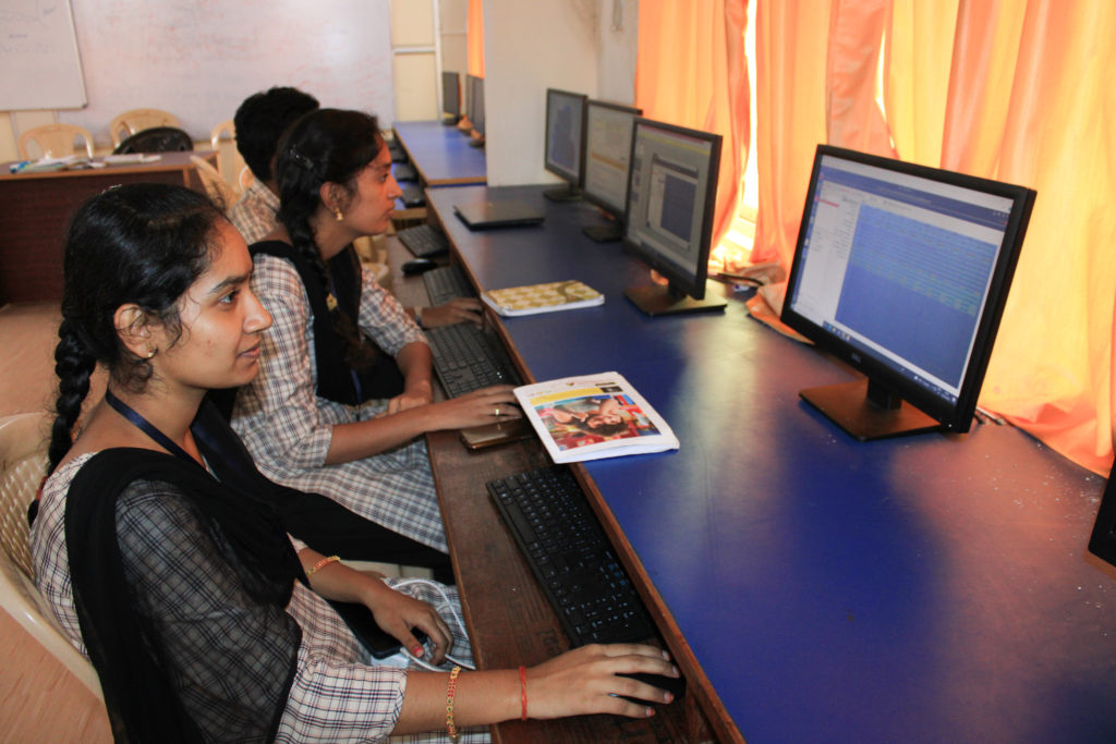
Ongoing Summer internship program on Processor Design from 16th May 2022 to 18th June 2022 @ CUTM, Odisha.
A group of 15 students enrolled for summer internship program in the field of Processor Design. This internship aims at making interns to understand Bluespec System Verilog programming with hands on in ASIC and FPGA Design and Implementation. Interns will become familiar with the use of Industry standard tools such as Cadence EDA Tool, BSV […]


Media


Our Main Teachers

Dr. Chandra Sekhar Dash currently works as Assistant Professor in the Department of Electronics and Communication Engineering at Centurion University of Technology and Management, Odisha. His research interests include Semiconductor Non-Volatile Memory (NVM) Technology and its Advanced Applications, Electronics Materials and VLSI Circuits. Dr. Chandra Sekhar Dash received his Ph.D and Masters from VIT University, […]
Satyanarayan Padhy currently working as Assistant Professor in the Department of Electronics and Communication Engineering at Centurion University of Technology and Management, Odisha. His research interests include Digital System Design,Signal Processing and Controller design for power converters. He has received his M.Tech from NIT, Allahabad, India in the Year 2013 and Currently Pursuing his PhD. […]

Sandipan Pine currently working as Associate Professor in the Department of Electronics and Communication Engineering at Centurion University of Technology and Management, Odisha. His research interests include Chip design and robotics area.He has received his M.Tech from IIT kharagpur in Microelectronics and VLSI and Currently Pursuing his PhD from Utkal University. He has published more […]